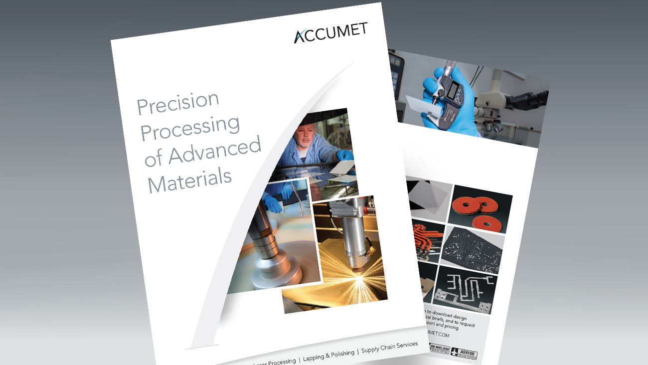
Precision Lapping of Ceramics and other Substrates for Electronics Manufacturing

Lapping is a machining process utilized to control a ceramic or other substrate's surface finish, thickness, parallelism, and flatness, and the process varies depending upon the type of material and the physical dimensions required. Accumet has developed several unique substrate lapping machining processes and we are the leaders in achieving extremely tight tolerances, while offering repeatability from piece to piece.
Lapping Tolerances
We are capable of achieving thickness tolerances as tight as ±0.000025" and surface finishes ranging from 5 micro-inches to 60 micro-inches. Material can be lapped down to as thin as .003'' with a tolerance as low as ± .0001''. Materials as large as 16'' square or diameter can easily be lapped. Flatness can be brought to within 0.0005'', depending upon overall size and thickness. And we are capable of holding these tolerances throughout the highest production volumes.
Depending upon the substrate material and customer requirements, different grades of grit, used at several different stages of manufacture are key. The substrate material, the grit of the abrasive, the ceramic machining technique, and lapping processing time are all contributing factors in achieving your parameters, and Accumet is the best in the world at it. This is evidenced by the faith put in us by the leading OEM's in RF/microwave microelectronics, aerospace, military and defense, semiconductor, and medical electronics industries.
TYPICAL LAPPING TOLERANCES
| Material | Virtually any type |
| Finish | Controlled finishes from 5 micro-inches to 60 micro-inches |
| Thinness Min. | Min. 0.003" with a tolerance to ± .0001'' |
| Thickness Tolerance | ±0.000025" (Industry standard tolerance = .0005") |
| Flatness | Can be held within the Helium light band range (11.6 millionths of an inch equals 1 band). Industry standard flatness is 0.0005" |
| Parallelism | Can be held within 0.000010" (ten millionths of an inch) |
We're located just north of Boston, Massachusetts in Devens, MA, and proudly service the entire US with many laser machining, secondary processing , and lapping and polishing services.


