Circuit Layout Design and the Pre-deposition
Posted on April 1, 2017 in Blogs

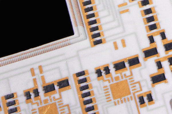
The design of your microelectronics circuit is a huge factor in determining whether its ceramic substrate can be laser cut. Here are some factors to consider as you design.
Almost every week it happens — an electronics component manufacturer asks if we can cut the ceramic substrate of a microelectronics circuit they have already designed. Of course we’re always happy to take a look. The problem is that by the time we see the design, decisions regarding size, shape, materials, feature layout, thickness, and other factors may have already been made. And some design decisions may make it impossible to laser cut the substrate as reliably, quickly, and as inexpensively as you might like.
So, if you’d like to know more about laser cutting ceramic substrates, here’s a quick overview:
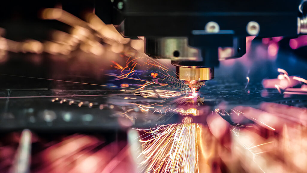
To reduce unit costs, parts are typically fabricated as a batch on an alumina ceramic sheet, which is then singulated into individual parts. Singulation is done in one of two ways. One way is to simply cut the parts out of the sheet. The other way is to laser pulse scribe lines between the parts and then mechanically snap the substrate along the scribe lines. (The scribe lines consist of tiny holes that, unlike a complete cut-through, only penetrate the sheet part way.) The laser may also drill holes (vias) in the substrate to allow metal connections to run between top and bottom.
The factors that you, as a designer, can control to make sure you obtain the desired cuts, include:
Part size: Ceramic substrates are brittle. Make them too big and they tend to break; too small and it becomes difficult to singulate them cleanly as individual parts. Factors such the amount of stress the part undergoes in the application and the distance between features on a sheet will affect size limitations (either too big or too small).
Distance between features on a sheet: You want to place features far enough apart so the distance from features to cut or scribe lines prevents damage to the parts during singulation. With cutting, damage can occur if the heat of the laser beam gets too close to the parts. With scribing, damage can occur from chipping — tiny pieces of ceramic breaking off too close to a feature when the substrates are snapped. The minimum distance from a cut line to a feature is .002″ versus a minimum of .005″ for a scribe line.
Materials: The most popular substrate materials are alumina, beryllium oxide (BeO), and aluminum Nitrate (AIN). Alumina 96% is used in 90% of the circuits in production today. However, alumina +99% offers a superior surface for fabricating thin-film circuitry. Where high heat conductivity is required, designers may choose beryllium oxide, or else aluminum nitride since it offers slightly less heat conductivity than BeO but is much easier to handle. Note also that surface metals can reflect laser light and cause the cut line width (kerf) to vary. Glass may tend to chip when cut, especially on the exit side of the laser beam.
Thickness: Lasers can typically cut sheets up to 1/8th inch thick. However, the thicker the sheet, the more powerful — hence, wider — the laser beam needed to cut through it. So a thicker substrate will yield fewer parts from the same size sheet.
Clearance inside curves: A big reason microelectronics designers prefer laser cutting to other methods is because lasers can cut ceramics into virtually any planer shape — circles, curves, rectangles, slit lines, and more. You just want to allow sufficient clearance around curves (at least 0.005 in. in radius) to avoid chipping where a feature should go. Rounding outside corners also reduces chipping.
Hole size and shape: When laying out features take into account that lasers produce tapered holes — the width at the entry point of the pulse is greater than at the exit point — the difference typically equal to 10% of the thickness of the material. A slightly longer focus lens will achieve smaller tapers.
If you want to specify other materials or exceed the dimensional limits recommended here, then you should probably talk to us first. In fact, you should probably talk to us first anyway.
To learn more about laser processing ceramic substrates download our tech brief, “5 Keys to Successful Laser Processing of Ceramic Substrates.”


